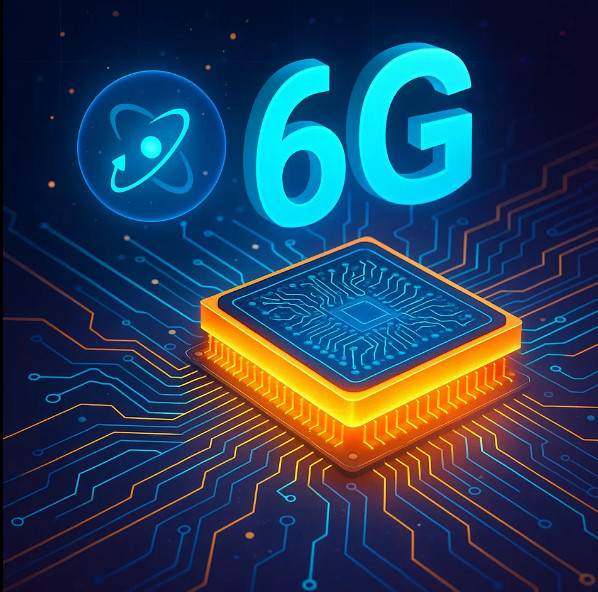
6G нҳҒлӘ…мқ„ мҳҲкі н•ҳлҠ” мҠӨн•ҖнҠёлЎңлӢүмҠӨ(spintronics) кё°л°ҳ л°ҳлҸ„мІҙ
кё°мЎҙ л°ҳлҸ„мІҙ кё°мҲ мқҳ л¬јлҰ¬м Ғ н•ңкі„лҘј лҸҢнҢҢ
5G мӢңлҢҖлҘј кІ¬мқён•ң кё°мЎҙ л°ҳлҸ„мІҙ, нҠ№нһҲ мӢӨлҰ¬мҪҳ кё°л°ҳ нҠёлһңм§ҖмҠӨн„°лҠ” кі мЈјнҢҢ мӢ нҳё м „мҶЎм—җм„ң м„ұлҠҘкіј м „л Ҙ нҡЁмңЁ л©ҙм—җм„ң м„ұмһҘмқҳ н•ңкі„м—җ м§Ғл©ҙн•ҳкі мһҲлӢӨ. мқҙмҷҖ лҢҖ비лҗҳм–ҙ м§Ҳнҷ”к°ҲлҘЁ(GaN) кё°л°ҳ мҶҢмһҗлҠ” лҚ” лҶ’мқҖ мЈјнҢҢмҲҳмҷҖ м „л Ҙ л°ҖлҸ„лҘј м ңкіөн•ҳм§Җл§Ң, кө¬мЎ°м Ғ н•ңкі„мҷҖ м—ҙ кҙҖлҰ¬ л¬ём ңлЎң мҷ„лІҪн•ң н•ҙкІ°мқҖ мқҙлЈЁм–ҙм§Җм§Җ лӘ»н–ҲлӢӨ. к·№лӢЁм ҒмңјлЎң л№ лҘё лҚ°мқҙн„° м „мҶЎ мҶҚлҸ„мҷҖ лӮ®мқҖ м§Җм—°мқҙ мҡ”кө¬лҗҳлҠ” 6G мӢңлҢҖлҘј мӨҖ비н•ҳкё° мң„н•ҙм„ңлҠ” м „нҳҖ мғҲлЎңмҡҙ л°ҳлҸ„мІҙ кө¬мЎ°мҷҖ мһ‘лҸҷ мӣҗлҰ¬к°Җ н•„мҡ”н•ҳлӢӨ. м—¬кё°м—җ мЈјлӘ©н•ң кІғмқҙ л°”лЎң мҠӨн•ҖнҠёлЎңлӢүмҠӨ кё°мҲ мқҙл©°, мқҙлҠ” кё°мЎҙ м „мһҗ мһҘм№ҳмқҳ вҖҳм „н•ҳвҖҷм—җ лҚ”н•ҙ вҖҳмҠӨн•Җ(spin)вҖҷмқҙлқјлҠ” м „мһҗмқҳ мһҗкё° лӘЁл©ҳнҠё(нҡҢм „н•ҳлҠ” мһҗкё°м Ғ м„ұм§Ҳ)лҘј нҷңмҡ©н•ҙ м •ліҙ мІҳлҰ¬мқҳ нҢЁлҹ¬лӢӨмһ„мқ„ к·јліём ҒмңјлЎң л°”кҝҖ мҲҳ мһҲлҠ” кё°мҲ мқҙлӢӨ.
мҠӨн•ҖнҠёлЎңлӢүмҠӨ кё°л°ҳ м§Ҳнҷ”к°ҲлҘЁ мҠҲнҚјлһҳнӢ°мҠӨ мәҗмҠ¬л ҲмқҙнӢ°л“ң м „кі„нҡЁкіј нҠёлһңм§ҖмҠӨн„°(SLCFETs) кө¬мЎ°
мҳҒкөӯ лёҢлҰ¬мҠӨнҶЁлҢҖн•ҷкөҗ м—°кө¬нҢҖмқҖ *л„ӨмқҙмІҳ мқјл үнҠёлЎңлӢүмҠӨ*м—җ л°ңн‘ңлҗң л…јл¬ём—җм„ң м§Ҳнҷ”к°ҲлҘЁ мҶҢмһ¬ кё°л°ҳм—җм„ң мҠҲнҚјлһҳнӢ°мҠӨ мәҗмҠ¬л ҲмқҙнӢ°л“ң м „кі„нҡЁкіј нҠёлһңм§ҖмҠӨн„° кө¬мЎ°лҘј лҸ„мһ…н•ҳмҳҖлӢӨ. мқҙ мһҘм№ҳлҠ” мҲҳмІң к°ңм—җ лӢ¬н•ҳлҠ” 100лӮҳл…ёлҜён„° мқҙн•ҳмқҳ вҖҳн•ҖвҖҷ кө¬мЎ°лҘј лі‘л ¬ л°°м№ҳн•ҳкі , м§Ҳнҷ”к°ҲлҘЁ лӮҙл¶Җмқҳ лһҳм№ҳ нҡЁкіјлқјлҠ” нҠ№м„ұмқ„ мғҲлЎӯкІҢ л°ңкІ¬н•ҳм—¬ кі мЈјнҢҢ мҰқнҸӯ м„ұлҠҘмқ„ к·№лҢҖнҷ”н•ңлӢӨ. лһҳм№ҳ нҡЁкіјлҠ” н•Җ нҳ•нғң кө¬мЎ°м—җм„ң м „лҘҳ м ңм–ҙк°Җ лҜјк°җн•ҳкІҢ мһ‘лҸҷн•ҳлҸ„лЎқ лҸ•лҠ” л¬јлҰ¬м Ғ нҳ„мғҒмңјлЎң, мқҙлҘј нҶөн•ҙ 75\~110кё°к°Җн—ӨлҘҙмё мқҳ W‑лҢҖм—ӯ мЈјнҢҢмҲҳм—җм„ң м „л Ҙ нҡЁмңЁмқ„ нҡҚкё°м ҒмңјлЎң лҶ’мқј мҲҳ мһҲлӢӨ. мқҙлҹ¬н•ң кө¬мЎ°м Ғ м„Өкі„лҠ” кё°мЎҙ лӢЁмқј мұ„л„җ нҠёлһңм§ҖмҠӨн„° лҢҖ비 м„ұлҠҘкіј м „л Ҙ нҡЁмңЁмқ„ лҸҷмӢңм—җ к°ңм„ н•ң мӮ¬лЎҖлЎң мЈјлӘ©л°ӣлҠ”лӢӨ.
мӢӨн—ҳ кІ°кіјмҷҖ кё°мҲ м Ғ м§„м „
мӢӨн—ҳм—җм„ңлҠ” мҠҲнҚјлһҳнӢ°мҠӨ мәҗмҠ¬л ҲмқҙнӢ°л“ң м „кі„нҡЁкіј нҠёлһңм§ҖмҠӨн„°к°Җ W‑лҢҖм—ӯ(75‑110кё°к°Җн—ӨлҘҙмё )м—җм„ң лҸҷмһ‘н•ҳлҠ” кі мЈјнҢҢ мҰқнҸӯкё°лЎңм„ң, 4.8A/mmкёүмқҳ м „лҘҳ л°ҖлҸ„мҷҖ 40% мқҙмғҒмқҳ м „л Ҙ мІЁк°Җ нҡЁмңЁмқ„ лӢ¬м„ұн–Ҳмңјл©°, 94кё°к°Җн—ӨлҘҙмё лҢҖм—ӯм—җм„ңлҠ” 10W/mm мқҙмғҒмқҳ м¶ңл Ҙмқҙ к°ҖлҠҘн•Ёмқ„ ліҙм—¬мЈјм—ҲлӢӨ. нҠ№нһҲ лһҳм№ҳ нҡЁкіјлҘј кІҖмҰқн•ҳкё° мң„н•ҙ 1,000к°ң мқҙмғҒмқҳ н•Җмқ„ к°ңлі„ мёЎм •н•ҳл©° нҠ№м • н•Җм—җм„ң м „лҘҳ кёүмҰқ нҳ„мғҒмқ„ нҸ¬м°©н–Ҳмңјл©°, 3D мӢң뮬л Ҳмқҙм…ҳкіј мһҘмӢңк°„ н…ҢмҠӨнҠёлҘј нҶөн•ҙ мқҙ нҡЁкіјк°Җ мһҘм№ҳмқҳ мӢ лў°м„ұкіј мҲҳлӘ…мқ„ н•ҙм№ҳм§Җ м•ҠмқҢмқ„ мһ…мҰқн–ҲлӢӨ. м Ҳм—°мёөмқҳ кі л¶„мһҗ мҪ”нҢ… лҚ•л¶„м—җ н•Җ к°„ к· мқјлҸ„к°Җ мң м§Җлҗҳкі м—ҙ м•Ҳм •м„ұмқҙ нҷ•ліҙлҗҳм—Ҳмңјл©°, кіјм—ҙ мӢң뮬л Ҳмқҙм…ҳм—җм„ңлҸ„ м§Ҳнҷ”к°ҲлҘЁ нҠ№м„ұмқҙ мң м§ҖлҗҳлҠ” кІғмқҙ нҷ•мқёлҗҳм—ҲлӢӨ. мқҙлҠ” мғҒмҡ©нҷ” к°ҖлҠҘм„ұмқ„ лҶ’мқҙлҠ” л§Өмҡ° мӨ‘мҡ”н•ң кІ°кіјлЎң нҸүк°ҖлҗңлӢӨ.
6GВ·мһҗмңЁмЈјн–үВ·мӣҗкІ© 진лЈҢ л“ұ мқ‘мҡ© нҷ•лҢҖ
мқҙ кё°мҲ мқҳ м Ғмҡ© к°ҖлҠҘм„ұмқҖ нҶөмӢ , мқҳлЈҢ, мһҗмңЁмЈјн–ү, мҙүк°Ғ н”јл“ңл°ұ л“ұ л§Өмҡ° кҙ‘лІ”мң„н•ҳлӢӨ. 6Gм—җм„ңлҠ” н…Ңлқјл№„нҠёкёү мҶҚлҸ„, мҲҳ л°ҖлҰ¬мҙҲ мқҙн•ҳ м§Җм—°, мҙҲкҙ‘лҢҖм—ӯ лҢҖм—ӯнҸӯмқҙ мҡ”кө¬лҗҳлҠ”лҚ°, мқҙлҠ” мғҲлЎңмҡҙ нҠёлһңм§ҖмҠӨн„° м•„нӮӨн…ҚмІҳ м—ҶмқҙлҠ” кө¬нҳ„мқҙ л¶Ҳк°ҖлҠҘн•ҳлӢӨ. лёҢлҰ¬мҠӨнҶЁ м—°кө¬нҢҖмқҖ мқҙлҹ¬н•ң кө¬мЎ°к°Җ 6G кё°м§Җкөӯ, мң„м„ұнҶөмӢ , м—Јм§Җ м»ҙн“ЁнҢ…, мһҗмңЁмЈјн–үм°Ё лқјмқҙлӢӨ л°Ҹ мӣҗкІ© мҲҳмҲ лЎңлҙҮ м ңм–ҙ л“ұм—җ н•„мҲҳм Ғмқё м„ұлҠҘмқ„ нҷ•ліҙн• мҲҳ мһҲмқҢмқ„ мӢңмӮ¬н•ҳмҳҖлӢӨ. нҠ№нһҲ лҢҖм—ӯнҸӯ мҰқлҢҖмҷҖ лҶ’мқҖ м „л Ҙ нҡЁмңЁмқҖ мһҗмңЁмЈјн–үм°Ё м„јм„ңмҷҖ мӣҗкІ© 진лЈҢ мһҘ비мқҳ мӢӨмӢңк°„ лҚ°мқҙн„° м „мҶЎмқ„ к°ҖлҠҘн•ҳкІҢ н•ңлӢӨ. мҙүк°Ғ н”јл“ңл°ұкіј к°ҷмқҖ мқёк°„-м»ҙн“Ён„° мғҒнҳёмһ‘мҡ© 분야м—җм„ңлҸ„ м „мҶЎ м§Җм—°мқ„ мӨ„м—¬ л°ҳмқ‘м„ұмқ„ лҶ’мһ„мңјлЎңмҚЁ мқёк°„ мҲҳмӨҖмқҳ мҙүк°җ н”јл“ңл°ұмқ„ мӢӨнҳ„н• мҲҳ мһҲлӢӨ.
мӮ°м—…м Ғ нҷ•мһҘм„ұкіј мғқнғңкі„ мҳҒн–Ҙ
мқҙ м—°кө¬м—җм„ңлҠ” лӢЁкё° мғҒмҡ©нҷ”лҘј лӘ©н‘ңлЎң м§Ҳнҷ”к°ҲлҘЁ кё°л°ҳ мҠҲнҚјлһҳнӢ°мҠӨ мәҗмҠ¬л ҲмқҙнӢ°л“ң м „кі„нҡЁкіј нҠёлһңм§ҖмҠӨн„°мқҳ м „л Ҙ л°ҖлҸ„мҷҖ мқён„°нҺҳмқҙмҠӨ м„Өкі„ кі лҸ„нҷ”лҘј м ңм•Ҳн•ҳмҳҖлӢӨ. л°ҳлҸ„мІҙ мӮ°м—…м—җм„ңлҸ„ м§Ҳнҷ”к°ҲлҘЁ кё°л°ҳ кі мЈјнҢҢ мҶҢмһҗлҠ” мқҙлҜё 5GмҷҖ м „л Ҙ м „мҶЎ 분야м—җм„ң л„җлҰ¬ мұ„нғқлҗҳкі мһҲмңјл©°, мқҙлІҲ кө¬мЎ°лҠ” кё°мЎҙ л°ҳлҸ„мІҙ м ңмЎ° кіөм •кіјлҸ„ 비көҗм Ғ нҳёнҷҳлҗҳл©° нҷ•мһҘ к°ҖлҠҘм„ұмқҙ лҶ’лӢӨ. мӮ°м—… нҢҢнҠёл„Ҳл“ӨмқҖ мқҙлҜё мғҒмҡ©нҷ”лҘј мң„н•ң нҸүк°Җм—җ м°©мҲҳн–Ҳмңјл©°, нӣ„мҶҚ м—°кө¬лЎң н•Җ л°ҖлҸ„ мҰқк°Җ, м—ҙ кҙҖлҰ¬ мөңм Ғнҷ”, м ңмЎ° кіөм • нҶөн•© л“ұмқҙ 추진лҗҳкі мһҲлӢӨ. мқҙлҠ” л°ҳлҸ„мІҙ кіөкёүл§қ, мӮ¬л¬јмқён„°л„·, нҶөмӢ мһҘ비 мғқнғңкі„ м „л°ҳмқҳ ліҖнҷ”лҘј мҙү진н•ҳкІҢ лҗ кІғмқҙлӢӨ. м—җл„Ҳм§Җ мҶҢ비 к°җмҶҢ, мЈјнҢҢмҲҳ нҡЁмңЁ к·№лҢҖнҷ”, мһҘм№ҳ мӢ лў°м„ұ н–ҘмғҒмқҖ кё°мҲ нҷ•мӮ°мқҳ н•өмӢ¬ м§Җн‘ңк°Җ лҗ кІғмқҙлӢӨ.
кіјм ңмҷҖ лҜёлһҳ м „лһө
м•„м§ҒмқҖ н”„лЎңнҶ нғҖмһ… мҲҳмӨҖмқҙл©°, мғҒмҡ© мһҘм№ҳлЎңмқҳ м „нҷҳмқ„ мң„н•ң мҲҳлӘ…В·мӢ лў°м„ұ н…ҢмҠӨнҠё, лҢҖлҹү мғқмӮ° кіөм • мөңм Ғнҷ”, мЈјнҢҢмҲҳ м•Ҳм •м„ұ мқёмҰқ, көӯм ң к·ңм ң л°Ҹ мғқнғңкі„ н‘ңмӨҖнҷ” л“ұмқҙ лӮЁм•„ мһҲлӢӨ. лһҳм№ҳ нҡЁкіј кё°л°ҳ мһҘм№ҳлҠ” м—ҙ л¶Җн•ҳмҷҖ мһҘкё° мһ‘лҸҷ м•Ҳм •м„ұ мёЎл©ҙм—җм„ң 추к°Җ кІҖмҰқмқҙ н•„мҡ”н•ҳл©°, 5GмҷҖмқҳ нҳёнҷҳм„ұкіј көӯм ң м „нҢҢ к·ңм ңлҘј 충мЎұн•ҙм•ј н•ңлӢӨ. лҸҷмӢңм—җ м§Ҳнҷ”к°ҲлҘЁ кё°нҢҗ м ңмЎ° нҷ•лҢҖ, нҢЁнӮӨ징 비мҡ© м Ҳк°җ, мғқмӮ° лӢЁк°Җ м Ҳк°җ м „лһө л“ұмқҙ лі‘н–үлҗҳм–ҙм•ј н•ңлӢӨ. к·ёлҹ¬лӮҳ мқҙ кё°мҲ мқҖ м—°кө¬м—җм„ң мғҒмҡ©к№Ңм§Җ 3\~5л…„ лӮҙ лҸ„м•Ҫ к°ҖлҠҘм„ұмқҙ мһҲмңјл©°, кёҖлЎңлІҢ л°ҳлҸ„мІҙ мӢңмһҘмқҳ кө¬лҸ„лҘј л’Өнқ”л“Ө мҲҳ мһҲлҠ” нҳҒмӢ мңјлЎң нҸүк°ҖлҗңлӢӨ.
мҠӨн•ҖнҠёлЎңлӢүмҠӨ кё°л°ҳ м§Ҳнҷ”к°ҲлҘЁ мҠҲнҚјлһҳнӢ°мҠӨ мәҗмҠ¬л ҲмқҙнӢ°л“ң м „кі„нҡЁкіј нҠёлһңм§ҖмҠӨн„°мқҳ мқҳмқҳ
кІ°лЎ м ҒмңјлЎң, лёҢлҰ¬мҠӨнҶЁлҢҖн•ҷкөҗ м—°кө¬нҢҖмқҳ мқҙлІҲ кё°мҲ мқҖ мҠӨн•ҖнҠёлЎңлӢүмҠӨ мӣҗлҰ¬мҷҖ лһҳм№ҳ нҡЁкіј кө¬мЎ° м„Өкі„мқҳ мңөн•©мқ„ нҶөн•ҙ нҶөмӢ мҶҚлҸ„мҷҖ м—җл„Ҳм§Җ нҡЁмңЁмқҳ кІҪкі„м„ мқ„ мһ¬м •мқҳн•ҳкі мһҲлӢӨ. мқҙлҠ” лӢЁмҲңнһҲ мғҲлЎңмҡҙ нҠёлһңм§ҖмҠӨн„°к°Җ м•„лӢҲлқј 6G мӢңлҢҖмқҳ м •ліҙкё°мҲ нҢЁлҹ¬лӢӨмһ„мқ„ л’·л°ӣм№Ён•ҳлҠ” кё°л°ҳ кё°мҲ мқҙлӢӨ. н–Ҙнӣ„ мһҗмңЁмЈјн–ү, мӣҗкІ© 진лЈҢ, мҙүк°Ғ н”јл“ңл°ұ л“ұ лҜёлһҳ мқ‘мҡ© 분야м—җм„ң мҠӨн•ҖнҠёлЎңлӢүмҠӨ кё°л°ҳ л°ҳлҸ„мІҙлҠ” мҙҲм Җм§Җм—°, кі мӢ лў°м„ұ, м Җм „л Ҙ нҠ№м„ұмқ„ нҶөн•ҙ мқёк°„ кІҪн—ҳмқ„ нҡҚкё°м ҒмңјлЎң н–ҘмғҒмӢңнӮӨлҠ” м—ӯн• мқ„ н•ҳкІҢ лҗ кІғмқҙлӢӨ.
* Reference
ScienceDaily, May 22, 2025, вҖңResearchers make breakthrough in semiconductor technology set to supercharge 6G delivery,вҖқ University of Bristol.
The Emergence of Spintronics‑Based Semiconductors Driving the 6G Revolution
Overcoming the Physical Limits of Conventional Semiconductors
Semiconductors that propelled the 5G era, particularly silicon‑based transistors, have now reached their limits in terms of high‑frequency signal transmission, performance, and power efficiency. Even GaN (gallium nitride)‑based devices, which offer higher frequency and power density, face inherent structural and thermal management issues. To meet the extreme demands of the 6G era—ultrafast data transfer speeds and ultra‑low latency—a fundamentally new semiconductor structure and operating principle is required. **Spintronics**, which utilizes not only the electronвҖҷs charge but also its spin (magnetic moment), emerges as a promising candidate. By leveraging this property, spintronics can redefine information processing paradigms at the physical level.
Spintronics‑Based GaN SLCFETs Structure
A research team at the University of Bristol introduced in *Nature Electronics* a new GaN‑based architecture called **SLCFETs (superlattice castellated field‑effect transistors)**. The device arranges thousands of sub‑100nm вҖңfinsвҖқ in parallel within GaN material and exploits a newly discovered property known as the вҖңlatch effectвҖқ to dramatically enhance RF amplification performance. This latch effect allows highly sensitive current control within the fin structures, enabling exceptionally high power efficiency in the W‑band frequency range (75–110 GHz). This architectural innovation simultaneously improves both performance and power efficiency, surpassing conventional single‑channel transistor designs.
Experimental Results and Technological Progress
In experiments, SLCFETs functioned as RF amplifiers operating in the **W‑band (75–110 GHz)**, achieving a current density of 4.8 A/mm and power‑added efficiency (PAE) exceeding 40%. At 94 GHz, it demonstrated output exceeding 10 W/mm. The researchers conducted detailed measurements across more than 1,000 fins and identified rapid current surges within individual fins—verifying the latch effect through extensive 3D simulations and long‑term tests. Notably, the addition of polymer coatings between fins ensured thermal stability and structural uniformity. These results point to strong commercial potential and operational reliability of the technology.
Expanding Applications in 6G, Autonomous Driving, Remote Healthcare
The applications of this technology extend across telecommunications, healthcare, autonomous driving, and tactile transmission. 6G networks will require terabit‑scale speeds, sub‑millisecond latency, and ultra‑wide bandwidth—all of which demand an entirely new transistor architecture. The Bristol team demonstrated that their SLCFETs design could power 6G base stations, satellite communication, edge computing, LIDAR for autonomous vehicles, and control of remote surgery robots. Enhanced bandwidth and high‑power efficiency will enable real‑time data transfer in autonomous vehicle sensors and medical equipment. In human interaction applications, such as tactile feedback, the reduction of transmission delay will enable human‑level responsiveness.
Industrial Scalability and Ecosystem Impact
The study proposes further optimization of **power density and interface design** for near‑term commercialization of GaN SLCFETs. GaN‑based RF components are already widely used in 5G and power transmission industries, and SLCFETs offer compatibility with existing manufacturing processes. Industry partners are now evaluating the technology for commercialization. Next steps include increasing fin density, optimizing thermal management, and integrating with semiconductor fabrication pipelines. The resulting improvements will significantly influence supply chains, the IoT ecosystem, and the communications hardware sector. Reducing energy consumption, maximizing frequency efficiency, and improving device reliability will be key drivers of adoption.
Challenges and Future Strategy
Currently in prototype stage, the technology must undergo further **lifetime and reliability testing** to transition to commercial products. Optimizing mass production processes, securing frequency stability certifications, and meeting international regulatory standards remain critical tasks. Additional work is needed to ensure long‑term thermal stability, ensure 5G compatibility, and meet global spectrum regulations. Scaling GaN substrate production, lowering packaging costs, and developing cost‑effective production models are parallel priorities. Nevertheless, the technology is projected to achieve commercial viability within **three to five years**, posing a significant challenge to established players in the global semiconductor market.
The Significance of Spintronics‑Based GaN SLCFETs
In conclusion, the University of BristolвҖҷs GaN SLCFETs technology—combining spintronics principles with latch‑effect architecture—redefines the boundaries of communication speed and power efficiency. It represents not merely a new transistor, but the foundation for **a new paradigm in 6G information technology**. Moving forward, spintronics‑based semiconductors will play a pivotal role in enhancing human experience through ultra‑low latency, high reliability, and low power characteristics in applications such as autonomous driving, remote healthcare, and tactile feedback transmission.
* Reference
ScienceDaily, May 22, 2025, вҖңResearchers make breakthrough in semiconductor technology set to supercharge 6G delivery,вҖқ University of Bristol.