мҙҲкі мҶҚ мҳҒмғҒ л°Ҹ н…Ңлқјн—ӨлҘҙмё (THz) нҺ„мҠӨ кё°л°ҳ нҶ нҸҙлЎңм§Җ мғҒнғң м ңм–ҙ
м–‘мһҗ л¬јм§Ҳ м ңм–ҙмқҳ кІҪкі„лҘј л„ҳм–ҙм„ңлӢӨ
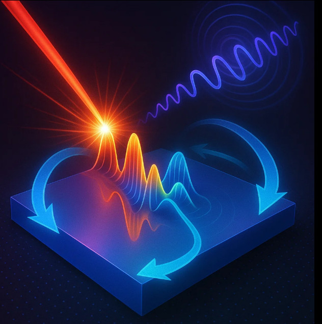
мҲҳмӢӯ л…„ лҸҷм•Ҳ л¬јм§Ҳ мғҒнғң м ңм–ҙлҠ” мҳЁлҸ„, м••л Ҙ лҳҗлҠ” нҷ”н•ҷм Ғ ліҖнҳ•м—җ мқҳмЎҙн•ҙ мҷ”лӢӨ. мқҙлҹ¬н•ң л°©лІ•л“ӨмқҖ лҠҗлҰ¬кі , к·№лӢЁм Ғмқҙл©°, лҢҖл¶Җ분 비к°Җм—ӯм Ғмқҙм—ҲлӢӨ. к·ёлҹ¬лӮҳ мҙҲкі мҶҚ л Ҳмқҙм Җ 분кҙ‘н•ҷмқҳ л“ұмһҘмңјлЎң кҙ‘н•ҷм Ғ м ңм–ҙ н•ҳм—җ м–‘мһҗ мғҒмқ„ мЎ°мңЁн•ҳлҠ” л№„м „мқҙ м ңмӢңлҗҳм—ҲлӢӨ. мөңк·ј мҠҲнҚјмҶҢлӢү м •л°Җ мЈјмӮ¬ н„°л„җл§Ғ нҳ„лҜёкІҪ(Scanning Tunneling Microscope, STM) нҢҒмқ„ нҶөн•ҙ лӢЁмқј мӮ¬мқҙнҒҙ н…Ңлқјн—ӨлҘҙмё (THz) нҺ„мҠӨлҘј лӢЁмёө н……мҠӨн…җ л””н…”лЈЁлқјмқҙл“ң(WTeвӮӮ)м—җ 집мҶҚн•ҳм—¬ мӣҗмһҗ мҲҳмӨҖ(м•Ҫ 7pm м •л°ҖлҸ„)м—җм„ң л¬јм§Ҳмқҳ 'нҶ нҸҙлЎңм§Җ мғҒнғң'лҘј м „нҷҳн•ҳлҠ” м—°кө¬лҠ” мӨ‘мҡ”н•ң мқҙм •н‘ңк°Җ лҗңлӢӨ.
м—¬кё°м„ң нҶ нҸҙлЎңм§Җ мғҒнғңлһҖ л¬јм§Ҳ лӮҙ м „мһҗмқҳ мӣҖм§Ғмһ„мқҙ мҷёл¶Җ нҷҳкІҪ ліҖнҷ”(мҳЁлҸ„, м••л Ҙ, кІ°н•Ё л“ұ)м—җлҸ„ мүҪкІҢ к№Ём§Җм§Җ м•ҠлҠ” 'м•Ҳм •м Ғмқё м „мһҗм Ғ м„ұм§Ҳ'мқ„ лң»н•ңлӢӨ. мқҙлҠ” л¬јм§Ҳмқҳ кІ°м • кө¬мЎ°мҷҖ м „мһҗмқҳ мғҒнҳёмһ‘мҡ©мңјлЎң мғқкё°лҠ” кі мң н•ң м–‘мһҗм Ғ нҠ№м„ұмңјлЎң, м „мһҗ нқҗлҰ„мқҳ мғҲлЎңмҡҙ кІҪлЎңлҘј л§Ңл“Өкұ°лӮҳ нҠ№м • м „мһҗ мғҒнғңлҘј мң м§Җн•ҳлҠ” лҚ° нҷңмҡ©лҗңлӢӨ. мҰү, мҷёл¶Җ көҗлһҖм—җлҸ„ мһҳ ліҙмЎҙлҗҳлҠ” вҖҳм–‘мһҗм Ғ ліҙнҳё мғҒнғңвҖҷлқјкі мқҙн•ҙн• мҲҳ мһҲлӢӨ.
мқҙлІҲ м—°кө¬лҠ” мҙҲкі мҶҚ кҙ‘н•ҷкіј мӣҗмһҗ мҲҳмӨҖ кіөк°„ 분н•ҙлҠҘмқ„ кІ°н•©н•ҳм—¬ мӢӨмӢңк°„ м „мһҗ мғҒ(phase) м ңм–ҙлҘј к°ҖлҠҘмјҖ н•ҳл©°, кё°мЎҙ л°©лІ•мңјлЎңлҠ” мғҒмғҒн• мҲҳ м—Ҷм—ҲлҚҳ к°ҖлҠҘм„ұмқ„ м—ҙм–ҙмЈјкі мһҲлӢӨ.
н…Ңлқјн—ӨлҘҙмё ‑STM мӢӨн—ҳ мһҘм№ҳ кө¬м„ұ
мқҙлІҲ м—°кө¬лҠ” мөңмӢ мЈјмӮ¬ н„°л„җл§Ғ нҳ„лҜёкІҪ мӢңмҠӨн…ңкіј мҙҲкі мҶҚ н…Ңлқјн—ӨлҘҙмё кҙ‘мӣҗ(single-cycle pulse)мқ„ нҶөн•©н•ҳм—¬ лӮҳл…ёлҜён„° мҠӨмјҖмқјмқҳ STM нҢҒ-мӢңлЈҢ м ‘н•©л¶Җм—җ м§Ғм ‘ м „лӢ¬н•ҳлҠ” кө¬мЎ°лЎң м„Өкі„лҗҳм—ҲлӢӨ. STM нҢҒмқҖ к·јм ‘мһҘ м•Ҳн…ҢлӮҳ м—ӯн• мқ„ н•ҳл©° мһҗмң кіөк°„мқҳ н…Ңлқјн—ӨлҘҙмё м „кё°мһҘ(м•Ҫ 20 V/cm)мқ„ м ‘н•©л¶Җм—җм„ң м•Ҫ 1 V/nm мҲҳмӨҖмңјлЎң мҰқнҸӯмӢңнӮЁлӢӨ. м—°кө¬м§„мқҖ мҙҲкі мҶҚ л Ҳмқҙм ҖмҷҖ н…Ңлқјн—ӨлҘҙмё л°ңмғқмқ„ лҸҷкё°нҷ”н•ҳм—¬ 200 fsмқҳ нҺ„мҠӨ нҸӯмқ„ лӢ¬м„ұн–Ҳмңјл©°, мӢңк°„ мҳҒм—ӯ 분кҙ‘лІ•мңјлЎң 0.26, 0.60, 2.24 н…Ңлқјн—ӨлҘҙмё л“ұ нҠ№м • мЈјнҢҢмҲҳ лҢҖм—ӯм—җм„ң л¬јм§Ҳмқҳ мҙҲкі мҶҚ мң м „ мқ‘лӢөмқ„ мёЎм •н•ҳмҳҖлӢӨ.
нҢҒ-мҰқк°• мӢ нҳё лҚ•л¶„м—җ н•ң мӮ¬мқҙнҒҙ мқҙн•ҳмқҳ мӢңк°„ н•ҙмғҒлҸ„лЎң м „лҘҳ ліҖнҷ”лҘј мҠӨлғ…мғ·мңјлЎң мәЎмІҳн• мҲҳ мһҲмңјл©°, мқҙлҘј нҶөн•ҙ мӢӨмӢңк°„ м „мһҗ лҸҷм—ӯн•ҷмқ„ 추м Ғн• мҲҳ мһҲлӢӨ. мқҙ мһҘм№ҳлҠ” лҳҗн•ң к·№м ҖмҳЁ мғҒнғңм—җм„ң н……мҠӨн…җ л””н…”лЈЁлқјмқҙл“ңмқҳ кІ°м • мғҒнғңлҘј к°Җм—ӯм ҒмңјлЎң м „нҷҳн•ҳл©ҙм„ңлҸ„ STM мқҙлҜём§ҖлҘј мӣҗмһҗ н•ҙмғҒлҸ„лЎң м ңкіөн•ңлӢӨ.
мӣҗмһҗ мҲҳмӨҖмқҳ нҶ нҸҙлЎңм§Җ мғҒнғң м „нҷҳ
н……мҠӨн…җ л””н…”лЈЁлқјмқҙл“ңлҠ” м „мқҙкёҲмҶҚ л””м№јмҪ”кІҢлӮҳмқҙл“ң лӢЁмёө л¬јм§ҲлЎң, кҙ‘м—җ мқҳн•ҙ кёҲмҶҚм„ұ лҳҗлҠ” л№„м •мғҒм Ғ мғҒнғңм—җм„ң м–‘мһҗ мҠӨн•Җ нҷҖ мғҒмңјлЎң м „мқҙн• мҲҳ мһҲлӢӨ. мқҙлІҲ м—°кө¬м—җм„ңлҠ” STM нҢҒмқ„ нҶөн•ң лӢЁмқј мӮ¬мқҙнҒҙ н…Ңлқјн—ӨлҘҙмё нҺ„мҠӨлҘј 집мӨ‘мӢңмјң мӣҗмһҗ мҲҳмӨҖ(м•Ҫ 7 Вұ 3 pm)м—җм„ң нҶ нҸҙлЎңм§Җ мғҒнғңлҘј к°Җм—ӯм ҒмңјлЎң м „нҷҳн•ҳлҠ” лҚ° м„ұкіөн–ҲлӢӨ. мқҙлҠ” лӘ…нҷ•н•ң мң„мғҒ м „нҷҳ нҠ№м„ұмңјлЎң лӮҳнғҖлӮ¬мңјл©°, STM м „лҘҳ мёЎм •мқ„ нҶөн•ҙ көӯмҶҢм Ғмқё м „мһҗ мғҒнғң л°ҖлҸ„ ліҖнҷ”лҘј нҷ•мқён•ҳмҳҖлӢӨ. мқҙ м „нҷҳмқҖ лӢЁмқј н…Ңлқјн—ӨлҘҙмё нҺ„мҠӨ мӮ¬мқҙнҒҙ лӮҙм—җм„ң л°ңмғқн•ҳл©°, м–‘мһҗ мғҒмқ„ мҙҲкі мҶҚмңјлЎң м ңм–ҙн•ҳлҠ” кІғмқҙ к°ҖлҠҘн•Ёмқ„ мһ…мҰқн•ҳмҳҖлӢӨ. мқҙлҠ” кҙ‘м—җ мқҳн•ҙ мң лҸ„лҗҳлҠ” лҢҖм№ӯм„ұ м „нҷҳмқҙлқјлҠ” кё°мЎҙ мқҙлЎ мқ„ мӢӨн—ҳм ҒмңјлЎң кІҖмҰқн•ң кІғмңјлЎң, м–‘мһҗ мғҒнғң м ңм–ҙмқҳ мғҲлЎңмҡҙ нҢЁлҹ¬лӢӨмһ„мқ„ м ңмӢңн•ңлӢӨ.
м„ңлёҢлӮҳл…ёлҜён„°, м„ңлёҢн”јмҪ”мҙҲмқҳ м–‘мһҗ м§ҖлҸ„ кө¬нҳ„
лӢЁмҲңн•ң мғҒнғң м „нҷҳмқ„ л„ҳм–ҙ н…Ңлқјн—ӨлҘҙмё ‑STMмқҖ л¬јм§Ҳмқҳ лҸҷм Ғ л°ҳмқ‘мқ„ мӢңкіөк°„ м–‘мһҗ м§ҖлҸ„(quantum landscape)лЎң мӢңк°Ғнҷ”н• мҲҳ мһҲлӢӨ. м—°кө¬м§„мқҖ н……мҠӨн…җ л””н…”лЈЁлқјмқҙл“ңмқҳ кІ°н•Ё л¶Җмң„м—җм„ң н…Ңлқјн—ӨлҘҙмё -мҰқк°• нҢҢнҳ•мқ„ мҲҳ집н•ҳм—¬ м„ңлёҢлӮҳл…ёлҜён„° кіөк°„ н•ҙмғҒлҸ„мҷҖ лӢЁмқј мӮ¬мқҙнҒҙ мқҙн•ҳ мӢңк°„ н•ҙмғҒлҸ„лЎң лҸҷм Ғ нҠ№м„ұмқ„ кҙҖм°°н•ҳмҳҖлӢӨ. мӢңк°„ мҳҒм—ӯ лҚ°мқҙн„°лҘј н‘ёлҰ¬м—җ ліҖнҷҳн•ҳл©ҙ лӢӨмӨ‘ н…Ңлқјн—ӨлҘҙмё лҢҖм—ӯм—җм„ңмқҳ мқҢн–Ҙ кіөлӘ… л°Ҹ н”ҢлқјмҰҲлӘ¬ к·јм ‘мһҘ мғҒнҳёмһ‘мҡ© м •ліҙлҘј лҸ„м¶ңн• мҲҳ мһҲлӢӨ. мқҙлҘј нҶөн•ҙ мӢӨмӢңк°„ лҸҷм Ғ н•„л“ң л°Ҹ мғҲлЎңмҡҙ м–‘мһҗ мғҒнғңмқҳ кіөк°„м Ғ ліҖнҷ”лҘј мӢңк°Ғм ҒмңјлЎң л§Өн•‘н• мҲҳ мһҲмңјл©°, мһҘм№ҳлҠ” мӢңлЈҢмқҳ кө¬мЎ°м Ғ ліҖнҷ”мҷҖ лҸҷм Ғ мқ‘лӢөмқ„ н”јл“ңл°ұ лЈЁн”„ нҳ•нғңлЎң 추м Ғн•ҳкІҢ лҗңлӢӨ.
м°Ём„ёлҢҖ лӮҳл…ём „мһҗ мһҘм№ҳмқҳ мқҙм •н‘ң
л№ӣл§ҢмңјлЎң л¬јм§Ҳмқҳ кІ°м • кө¬мЎ°мҷҖ м „мһҗ нҶ нҸҙлЎңм§ҖлҘј м ңм–ҙн•ҳлҠ” кІғмқҖ кё°мЎҙ л¬јлҰ¬н•ҷмқ„ лӣ°м–ҙл„ҳлҠ” нҢЁлҹ¬лӢӨмһ„мқҳ ліҖнҷ”лӢӨ. мқҙлҹ¬н•ң л№„м ‘мҙүмӢқ мҙҲкі мҶҚ м ңм–ҙлҠ” м–‘мһҗ мҠӨмң„м№ҳ, нҶ нҸҙлЎңм§Җ л©”лӘЁлҰ¬, мҙҲм Җм „л Ҙ м–‘мһҗ л…јлҰ¬ кІҢмқҙнҠё к°ңл°ңлЎң мқҙм–ҙм§Ҳ кІғмқҙлӢӨ. н……мҠӨн…җ л””н…”лЈЁлқјмқҙл“ңм—җм„ң мһ…мҰқлҗң мӣҗмһҗ мҲҳмӨҖмқҳ м •л°Җм„ұкіј мҙҲкі мҶҚ м ңм–ҙлҠ” кё°мЎҙ м „мһҗ мһҘм№ҳлҘј л„ҳм–ҙ, мөңмҶҢ м—җл„Ҳм§Җ мҶҗмӢӨлЎң лҸҷмһ‘н•ҳлҠ” мӣҗмһҗ нҒ¬кё° м ‘н•©л¶ҖлҘј кө¬нҳ„н•ҳлҠ” лҚ° кё°м—¬н• кІғмқҙлӢӨ. лҳҗн•ң мқҙлҠ” мҷҖмқј л°ҳкёҲмҶҚ, к°•мң м „мІҙ, мҙҲм „лҸ„мІҙ, мһҗм„ұмІҙ л“ұ лӢӨм–‘н•ң м–‘мһҗ л¬јм§Ҳм—җ мқ‘мҡ©лҗ мҲҳ мһҲмңјл©°, м–‘мһҗ лӮҳл…ём „мһҗкіөн•ҷкіј м–‘мһҗм •ліҙ мӢңмҠӨн…ң к°ңл°ңм—җ нҸӯл„“мқҖ к°ҖлҠҘм„ұмқ„ м—ҙм–ҙмӨ„ кІғмқҙлӢӨ.
лҸ„м „ кіјм ңмҷҖ мӢӨмҡ©нҷ”лҘј н–Ҙн•ң м „лһө
н…Ңлқјн—ӨлҘҙмё ‑STM кё°мҲ мқҖ нҳ„мһ¬к№Ңм§ҖлҠ” мҙҲкі м§„кіө(UHV)кіј к·№м ҖмҳЁ нҷҳкІҪм—җм„ңл§Ң мӢӨн—ҳмқҙ к°ҖлҠҘн•ҳлӢӨ. мқҙлҘј мғҒмҡ© мҶҢмһҗм—җ нҶөн•©н•ҳкё° мң„н•ҙм„ңлҠ” мҳЁм№© н…Ңлқјн—ӨлҘҙмё кё°мҲ к°ңл°ң, MHz мқҙмғҒмқҳ л°ҳліөлҘ н–ҘмғҒ, мң„мғҒ м•Ҳм •нҷ”, мһҘкё° лҸҷмһ‘ м•Ҳм •м„ұ кІҖмҰқмқҙ н•„мҡ”н•ҳлӢӨ. м—ҙ кҙҖлҰ¬, нҢЁнӮӨ징 кё°мҲ , мЈјліҖ нҷҳкІҪ м•Ҳм •м„ұ л¬ём ңлҸ„ н•ҙкІ°н•ҙм•ј н•ңлӢӨ. к·ёлҹ¬лӮҳ мҙҲкі мҶҚ лҢҖм№ӯм„ұ м „нҷҳ мқҙлЎ кіј мқҙлІҲ мӢӨн—ҳм—җм„ң м ңмӢңлҗң м„ұлҠҘ м§Җн‘ңлҠ” мқҙлҹ¬н•ң м ңм–ҙ мӣҗлҰ¬лҘј мӢӨлҰ¬мҪҳ нҡҢлЎңлӮҳ м–‘мһҗ м„јм„ң н”Ңлһ«нҸјмңјлЎң мқҙм „н• мҲҳ мһҲлҠ” к°ҖлҠҘм„ұмқ„ мһ…мҰқн•ҳкі мһҲмңјл©°, н–Ҙнӣ„ 5\~10л…„ лӮҙ мғҒмҡ©нҷ”к°Җ мқҙлЈЁм–ҙм§Ҳ кІғмқҙлӢӨ.
л№ӣмңјлЎң м ңм–ҙн•ҳлҠ” м–‘мһҗ л¬јм§Ҳ мӢңлҢҖмқҳ лҸ„лһҳ
лӢЁмёө н……мҠӨн…җ л””н…”лЈЁлқјмқҙл“ңм—җм„ң мһ…мҰқлҗң н…Ңлқјн—ӨлҘҙмё нҺ„мҠӨ кё°л°ҳ мӣҗмһҗ мҲҳмӨҖ нҶ нҸҙлЎңм§Җ мғҒнғң м „нҷҳмқҖ мғҲлЎңмҡҙ кё°мҲ м Ғ м§ҖнҸүмқ„ м—ҙм—ҲлӢӨ. мқҙлҠ” лӢЁмҲң мёЎм •мқҙ м•„лӢҲлқј л№ӣмңјлЎң л¬јм§Ҳмқҳ к·јліём Ғ м–‘мһҗ мғҒнғңлҘј м ңм–ҙн•ҳлҠ” кё°мҲ лЎңм„ң, кё°мЎҙмқҳ м •м Ғмқё л¬јм§Ҳ к°ңл…җмқ„ л„ҳм–ҙ вҖҳлҸҷм Ғмқҙкі к°Җм—ӯм Ғмқё мғҒнғң м ңм–ҙвҖҷк°Җ к°ҖлҠҘн•Ёмқ„ ліҙм—¬мӨҖлӢӨ. мқҙлҹ¬н•ң кё°мҲ мқҖ н–Ҙнӣ„, л№ӣмқҳ нҢҢнҳ• л§ҢмңјлЎң нҶ нҸҙлЎңм§Җм Ғ м§Ҳм„ңлҘј м ңм–ҙн•ҳкі , мӢӨмҳЁм—җм„ңлҸ„ мӣҗмһҗ н•ҙмғҒлҸ„лЎң мҙҲкі мҶҚ м „нҷҳмқ„ кө¬нҳ„н•ҳлҠ” мғҲлЎңмҡҙ м–‘мһҗ мӣҗмІң кё°мҲ лЎң л°ңм „н• кІғмқҙлӢӨ.
* Reference
arXiv, November 12, 2024, вҖңTerahertz control of surface topology probed with subatomic resolution,вҖқ Vedran Jelić et al.